
Solar cell construction has several stages. The p region is thin enough to allow light to enter the material and diffuse into the n-region. The n material is thin and has holes that diffuse light towards the junction. The bottom portion of the n–material is coated with metal. The two components are attached in a series and are surrounded by a glass window.
Pn-junction solar cell
The Pn-junction cell is composed of three layers: the top, absorber, and back junction. The top junction is made of silicon, while the absorber layer is composed of a thin layer of P material. This allows incident photons to pass through the junction. Photons cause electrons to be released from their parent atoms. This creates free electrons and holes at both ends of the junction. A current can flow when light causes electrical charges to change in cells' layers. The current is directly proportional the area that has been illuminated. The amount of light that the cell receives determines the open circuit voltage.
The p-n Junction is made up of two layers. They are laid so that electrons from one layer can move towards the other and fill in holes near the junction. This makes the p junction look like a tiny battery cell and sets up a photovoltage. The p-n Junction creates a tiny current when a small load is applied to it.
Single-junction silicon solar cell
Single-junction silicon solar cells use two layers of silicon, the lower layer containing a lower number of electrons, and the upper layer containing a higher number. The lower layer can be called positive-type, and the higher layer is negative. The p-n junction connects these two layers, causing a current to flow.
For decades, single-junction solar cells were extensively studied. Their practical efficiency has been improved to 26% under 1-sun conditions. You can further improve their efficiency by adding them to cells with large bandgap energetics. These convert short-wavelength photos and generate more voltage. Dual-junction cells may also be used to reduce thermalization losses. They can also produce high external-radiative efficiency.
Solar cells can be used in series-parallel combinations
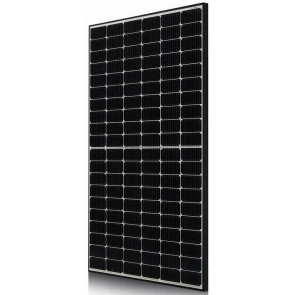
The series-parallel combination (or series) of solar cells can boost the voltage or electric current produced by them. This combination is used to make solar panels. One solar cell is connected in series parallel to create a single module. The modules are then joined together to form the solar array.
The area of a sun-powered solar cell directly affects its ability to produce electricity. Larger cells will produce more electricity. These quantities are measured using the short-circuit current, Isc, and the current density (Jsc). The voltage and current density are generally proportional to the short-circuit potential.
Reflective layer
A reflective layer placed on a solar cells can increase energy generation. This is a thin layer made of material that acts like a barrier between the semiconductor's and the air. The layer is usually made of a material with a refractive index of the same as the semiconductor. The film can reflect light in two directions. An AR layer of high quality will reduce the reflection points.
The reflective layer, which is the last layer on a solar panel, is called the reflective layer. It is responsible for reducing light loss. Various materials are used for this purpose, depending on the application and cost.
Base layer
The silicon is used in the base layer of a sun-powered cell. It is an antireflection layer that reduces light loss through reflection and encourages light transmission to energy-conversion layers. This layer is often made from silicon oxides, tantalum or titan and is formed with a spin coating or vacuum deposition.
The solar cell's bottom layer absorbs light with high efficiency. It is composed of two layers: the n-type and p-type. The n type silicon layer is composed of fewer positively charged holes (called “vacancies”), while the p type silicon contains many negatively charged electrons. The absence of valence elements causes vacancies. This leads to the movement of electrons from one side of the junction to the opposite side. This phenomenon is known as the depletion area.